Why is it Impossible to Mount the Crystal Oscillator on the PCB's Edge?

During the test, a driving recorder must be linked through an external adapter. When the machine is turned on and tested, it is discovered that the radiation is above the acceptable level. They are 84MHz, 144MHz, and 168MHz, respectively. Analyzing the root cause of the high radiation is required in order to provide appropriate countermeasures. These are the results of the radiation test:
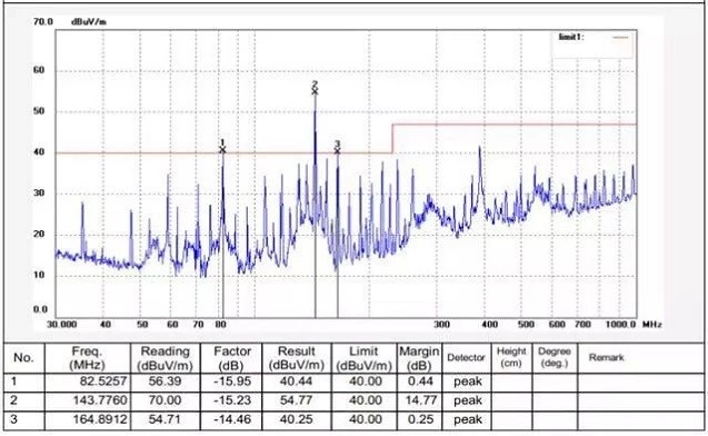
Figure 1 Radiation Test Data
Radiation Source Analysis
There is only one PCB in the device (kindly check on easybom), and it has a 12MHz crystal. The multiplier of 12MHz is one of the over-standard frequency points among them, and analysis of the screen and camera of the machine that is susceptible to EMI radiation above the standard reveals that the LCD-CLK is 33MHz and the camera MCLK is 24MHz. Through exclusion, it is discovered that the over-standard point remains even when the camera is removed. It is determined that the 144MHz exceeding point is related to the crystal since shielding the 12MHz crystal reduces the exceeding point, and the PCB layout is as follows:
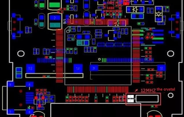
Figure 2 PCB Layout Diagram
The Principle of Radiation Generation
The PCB layout shows that the 12MHz crystal is positioned right on the board's edge. The high-speed device of the product being tested will form a specific capacitive coupling with the reference ground in the laboratory when it is placed in the radiation emission test environment. This capacitive coupling results in parasitic capacitance, which causes common-mode radiation. The stronger the parasitic capacitance, the more powerful the common-mode radiation, according to easybom. The essence of parasitic capacitance is the electric field distribution between the crystal and the reference ground. The distribution of the electric field between the two when the voltage is constant. The parasitic capacitance increases as the electric field strength between the two increases. The electric field distribution is as follows when the crystal is on the PCB's edge and in the center:
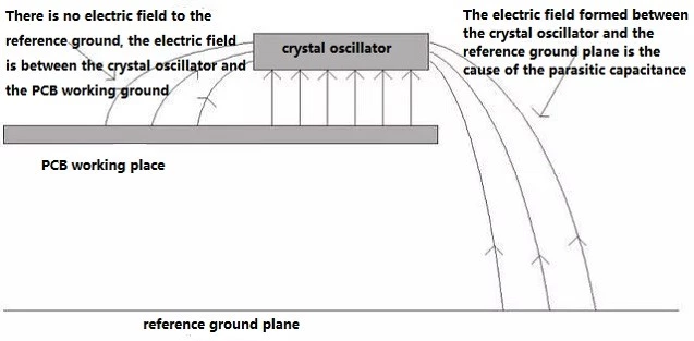
Figure 3 Schematic Diagram of the Electric Field Distribution Between the Crystal Oscillator at the Edge of the PCB and the Reference Ground Plane
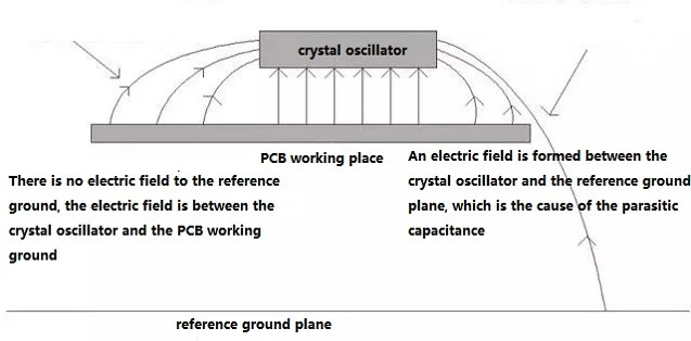
Figure 4 Schematic Diagram of the Electric Field Distribution Between the Crystal Oscillator in the Middle of the PCB and the Reference Ground Plane
The working ground (GND) plane in the PCB allows the crystal oscillator to control the majority of the electric field, which means that inside the PCB, the electric field distributed to the reference ground plane is significantly reduced, resulting in reduced radiated emissions. This can be seen in the figure when the crystal oscillator is placed in the middle of the PCB or far from the edge of the PCB.
Treatment Options
Apply copper to the PCB surface within 1 cm of the crystal oscillator, and link the copper on the surface layer to the PCB ground plane through holes. Move the crystal oscillator inward so that it is at least 1 cm from the edge of the PCB. The amended test result's spectrogram is shown below; it is clear from the image that the radiated emission has greatly improved.
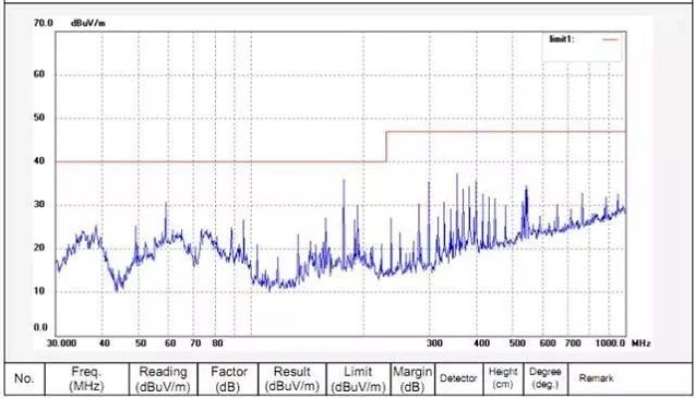
Figure 5
Contemplation and Enlightenment
Sensitive printed lines or devices positioned on the edge of the PCB will result in immunity issues, and capacitive coupling between high-speed printed lines or devices and the reference ground plane will result in EMI issues.
A working ground wire can be placed on the edge of the printed line if the design must be placed on the edge of the PCB for other reasons, and additional vias are added to connect the working ground wire to the working ground plane.


Abdur Rehman, PE
Author
Abdur Rehman is a professional electrical engineer with more than eight years of experience working with equipment from 208V to 115kV in both the Utility and Industrial & Commercial space. He has a particular focus on Power Systems Protection & Engineering Studies....
He earned his BSEE & MSEE from Washington State University in 2013 & 2017 respectively and an Engineering Technology Management degree in 2021.
Abdur Rehman is the CEO and co-founder of allumiax.com and creator of GeneralPAC by AllumiaX. He has been actively involved in various roles in the IEEE Seattle Section, IEEE PES Seattle, IEEE Region 6, and IEEE MGA.
Abdur Rehman is a board member of CordobaAcademy.org and enjoys local community volunteering. All AllumiaX blogs are special because of his love to share knowledge in the most intuitive way possible.
Stay Sharp & Join our Mailing List!
Subscribe to Allumiax Blog for updates on power system studies, tips, guides and insights on electrical engineering from industry leaders.

Recent Posts
Stay Sharp & Join our Mailing List!
Subscribe to Allumiax Blog for updates on power system studies, tips, guides and insights on electrical engineering from industry leaders.